Challenges

Optical testing solutions for universities and labs
Explore our industry-leading portfolio of optical testing solutions for universities and laboratory applications. This brochure provides an overview of our comprehensive range of optical testing solutions including component test platforms, optical testing solutions, light sources, benchtop tunable lasers, passive component testers, optical spectrum analyzers, tunable filters with adjustable bandwidth, variable attenuators, switches and power meters.
Description
Driving the development of high-speed networks and 5G, photonic integrated circuits (PICs) are a well-known technology in the telecom world—mainly thanks to the frantic development of transceivers and passive components that are smaller, faster, cheaper and greener than their bulk-optics counterparts. PICs are also getting traction—both from a commercial and research perspective—in other sectors too (e.g., lab-on-a-chip, LIDAR technology or quantum computing).
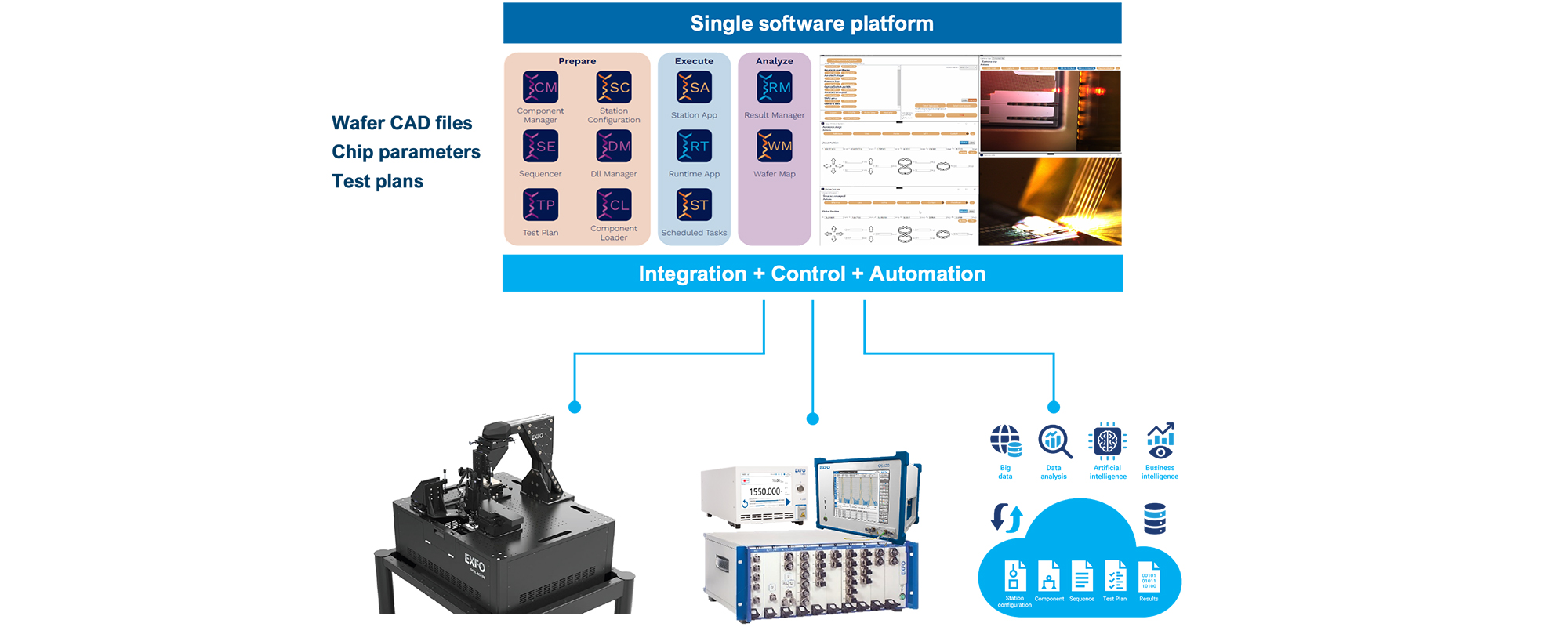
EXFO has worked closely with this fast-paced PIC industry and community over the years to develop test and measurement (T&M) hardware and software solutions that are automated, scalable, fast, accurate and cost-optimized. These solutions range from simple optical testing to spectral optical characterization or traffic analysis. EXFO also offers an extensive selection of probe stations for wafer, bar, multi-die or single die configurations, and a powerful automation software suite.
Through memberships in consortiums, EXFO has partnered with major vendors worldwide to offer integrated solutions for testing PICs.

New technology, new challenges
The rise of integrated photonics brings complex, new challenges in R&D and in the maturation iterations towards the commercial success of a product. Testing is a critical aspect, as it represents most of the cost of the product and its outputs are consumed at all life cycle stages—from design and development, through qualification and validation to production.
Automation is key in this regard. However, repeatability, scalability and parallelization of the testing processes are also needed for the massive volume of circuits and ports, in view of meeting the profitability of economies of scale that photolithography fabrication promises.
It can also be tricky to keep up with evolving optical test requirements and to equip photonics labs accordingly for testing active (i.e., emitting light) or passive (i.e., guiding light) optical components. You may be asking yourself: what spectral testing capabilities should I be looking for right now or in the near future? How can I obtain traffic analysis for PICs? Read on to explore solution avenues.
Automate and accelerate testing for PIC and optical components, from design to test and validation

Design and manufacturing of PIC dies is maturing fast, with photonic wafers now containing thousands of components made available by foundries through process design kits (PDKs). To create and update these PDKs, wafer manufacturers require reliable testing solutions to optimize the different parameters of interest for a given optical component.
Testing is a crucial step after design and manufacturing to provide feedback to the design tools and help optimize them. It is also needed for process control, to ensure that devices operate as expected throughout the assembly and packaging of the PIC chips. The PIC devices are usually tested at the wafer level prior to dicing so as to detect defects as early as possible and to avoid packaging defective dies.
Using a PIC wafer probe station, light can be coupled in and out of each chip using specially designed optical fiber hardware and high-precision alignment software. It is also possible to couple several components simultaneously using a fiber array. Precision alignment and speed allow coupling optimization within a fraction of a second.
Once the light is coupled into the wafer, the optical characteristics of the DUT can be measured. Testing photonic devices is at the heart of EXFO’s expertise; the CTP10 specifically addresses key PIC measurement challenges. EXFO's PIC testing solutions can measure optical components quickly, reliably and accurately.
EXFO Pilot software – Edge coupling on a single die
Automated probe stations
The OPAL series of automated probe stations is designed for industry-leading performance in testing wafers, multiple dies, or single dies in integrated photonics. With trench coupling capabilities and reconfigurable options, they ensure precise, repeatable, and fast measurements.
Flexible testing of photonic integrated circuits (PIC)
The OPAL series provides versatile PIC testing solutions, with various models designed to meet the specific needs of single-die, multi-die, and wafer-level edge-coupling applications.
OPAL-SD: An entry-level, semi-automated probe station for single-die testing. It offers flexible, cost-effective, and upgradeable performance, with automated optical alignment and traceable test results. Manual positioning of the die and electrical probes makes it a practical solution for precision testing.
OPAL-MD: A high-performance multi-die test station, delivering fast, accurate, and repeatable results. It’s designed for advanced integrated photonics characterization and allows for flexible testing setups. Open to EXFO and third-party instruments, the OPAL-MD supports comprehensive, data-driven PIC testing.
OPAL-EC: A leading-edge wafer-level test station optimized for edgecoupling. It provides industry-leading accuracy, speed, and flexibility for integrated photonics characterization. The OPAL-EC is ideal for precise wafer-level PIC testing, combining EXFO's optical measurement capabilities with compatibility for third-party instruments.

Testing passive components
Testing PIC-based passive components is often challenging due to the high port count of some components like arrayed waveguide grating (AWG) or the sheer number of components to test on a single die. A component test platform is a multiport detection system that operates in conjunction with a continuously tunable laser to measure optical insertion loss, return loss and polarization-dependent loss across the laser’s spectral range. The method yields optical spectrum quickly and with a high wavelength resolution, typically on the order of a picometer.
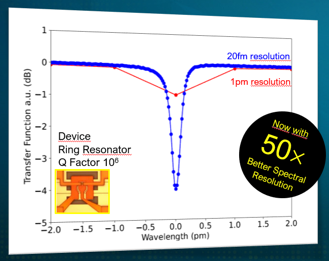
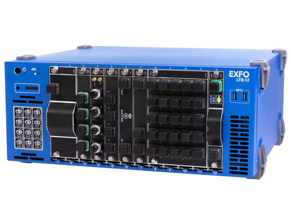
The CTP10 is a modular component test platform that operates together with the T200S or T500S continuously tunable lasers. The CTP10 characterizes the spectral properties of high port count devices in one single scan with high spectral resolution and a 70-dB dynamic range, even at a sweep speed of 200 nm/s. The CTP10 operates from 1240 to 1680 nm and covers a wide range of applications, including telecom, sensing and LIDAR. The instrument allows for both optical and photocurrent measurements with analog output possible for PIC first-light search and coupling optimization. Its electronics and internal processor make data transfer a breeze. The CTP10 can be remotely controlled using SCPI commands, facilitating integration as part of an automated PIC testing setup, increasing PIC testing throughput while reducing test time. The high sampling resolution down to 20 fm of the CTP10 enables the accurate measurement of narrow spectral features, such as the resonances of high-Q ring resonators (see example below), that have applications in modulators and sensors.
For the characterization of PIC components with a limited number of outputs, the CT440 is a more compact solution. The CT440 has the same wavelength accuracy and spectral coverage as the CTP10 and can perform IL/PDL measurements.
Reconfigurable tests
When testing hundreds or even thousands of components on a single wafer, automation quickly becomes essential. This is particularly the case considering that optical functionalities may vary from device to device or from die to die. As a result, PIC test solutions need to address fast reconfiguration of port connectivity using automated optical switches. Additionally, simpler, single-point tests may also be beneficial to the overall speed of the test and measurement (T&M) process.
EXFO’s solutions address this challenge from two angles. First, through optical testing building blocks (FTBx modules) for a simple laser + power meter test configuration with the possibility of adding attenuators, switches or different types of optical sources. Second, rapid yet repeatable reconfiguration with the MXS matrix switch.
Related resources :
PIC-based transceivers: Traffic analysis
Photonic integrated circuits are currently being deployed to tackle the bandwidth stress taking place in the transceiver industry. This stress is due to ever-increasing performance demands and costs pressures experienced by data centers and 5G applications.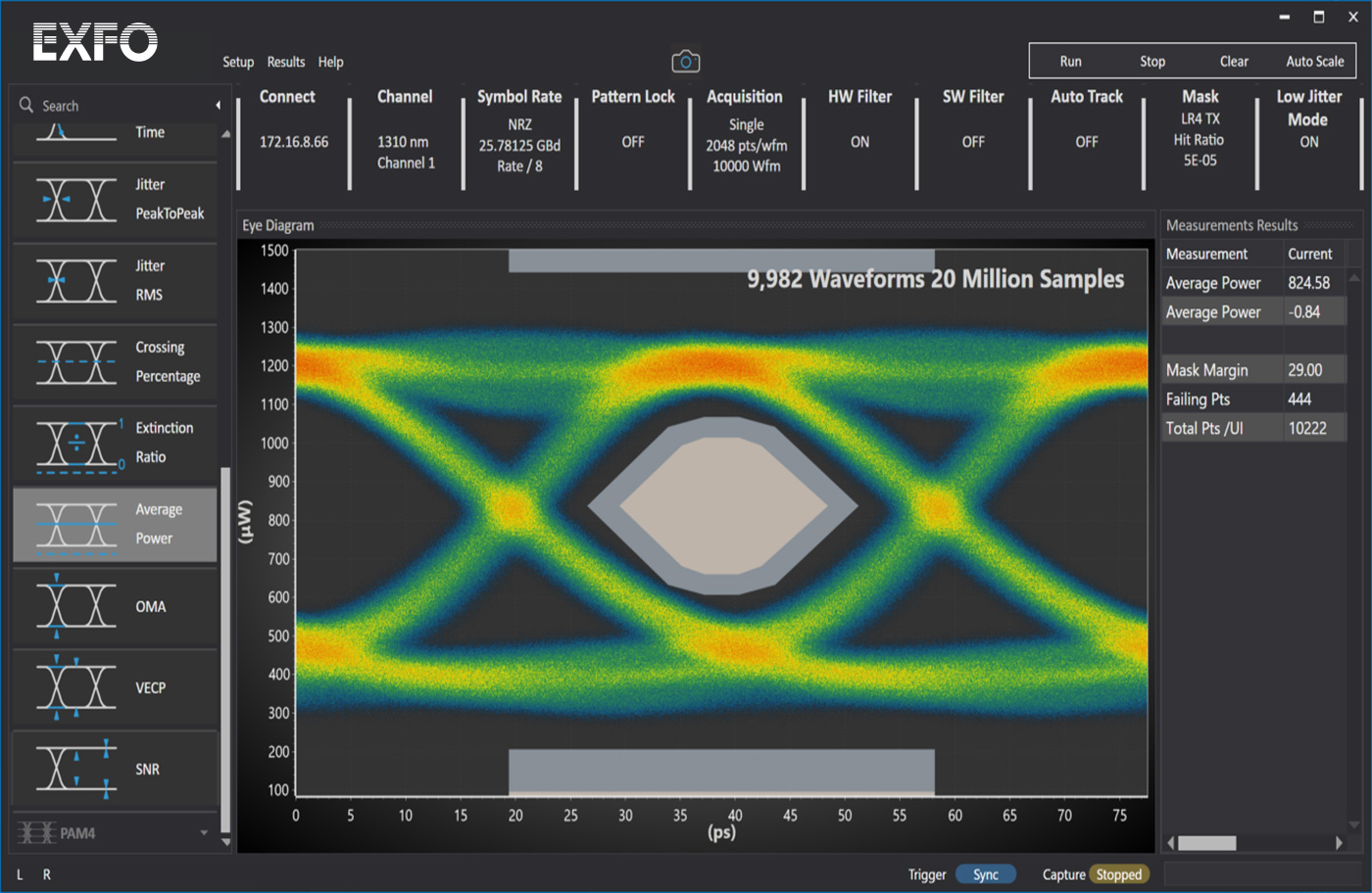
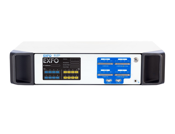
End-to-end transceiver qualification requires an entire range of high-end optical and electrical testers. To help transceiver vendors ensure compliance throughout the transceiver lifecycle, EXFO offers a range of electrical and optical testing solutions from wafer-level to packaged devices, including the EA-4000 sampling scope and the BA-4000 bit error rate tester.
To learn more about bit-error-rate testers and sampling scopes, download and browse our flyer.

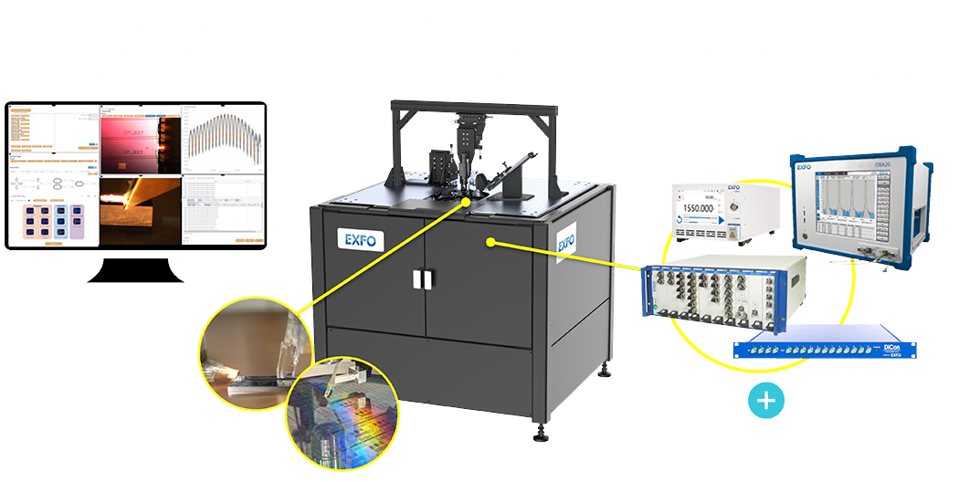
Data-driven test automation
The EXFO Pilot software suite enhances all OPAL stations by automating the test flow from setup to results analysis, turning high-quality measurements into actionable data for efficient and data-driven decision-making.
Key benefits
Improve production yield with R&D-grade solutions that rapidly provide best-in-class measurements.
EXFO offers a wide range of optical and electrical testing instruments for customized turnkey solutions that can evolve with your needs.
EXFO is actively involved in multiple partnerships with key hardware and software companies in the PIC ecosystem to validate interoperability.


